Thursday, November 20, 2014

NE555 Touch Switch

The series of touch switch or touch switch is built by IC NE555, a series of touch switches can be used to turn on lights, alarms or other electronic equipment. This circuit uses 2 pieces of metal plate media as touch, MP1 (Metal Plate 1) and MP2 (Metal Plate 2). Touch switch circuit is equipped with a visual LED indicator for relay status (load active). To enable (Relay ON) can be done by touching the surface of MP1 and to turn it off by touching the surface of the MP2. MP1 and MP2 in touch this switch can use a small piece of copper (diameter 5mm) was enough.

Touch Switch series with NE555.
555


Component List 555 touch Switch
R1 = 3.3M
R2 = 3.3M
R3 = 10K
R4 = 1K
C1 = 10nF-63V
D1 = 1N4007
D2 = Red LED
Q1 = BC547
IC1 = NE555
RL1 = 12V Relay
Read More..

Solve buzzing and noise on the amplifier circuit

Power amplifiers that we sometimes raises a raft of small drone as groundingless than perfect.The following are some ways to cope with the hum of the power amplifier: 

1. Keep sensitive circuits of the transformer, casing dimensions are not too small.One blog even suggested to use two-bok, bok special one for the transformer. For the toroid transformer or amplifier with a large transformer, should only contain a series of power amps, with no tone control. 
2. Change the position of the transformer, side by side into the lower side (the transformer is high) withfacing a series of sensitive posts 
3. Use a spacer on each PCB board as high as half the height of the transformer, eg as high as 2.5 cm or more so that the PCB board parallel to the core / center of the transformer, here the effect of the weakest fields. 
4. We recommend using a stereo module instead of two mono modulesThis avoids wiring errors. If forced to, try to sizecable between the right and left modules as long and as short as possible. 
5. Should take the ground path for the speaker of ct ct elco instead of the transformer,if the board pcb mounted two big elco (like elco power supply), takeground path of the speakers here, and check to hear! 
6. Power supply for radio (TX or RX) is very sensitive, use a capacitor4x100nf, 4 pairs of these capacitors in parallel to each mem-diode (bridge). 
7. At the tone control circuit IC op-amp that uses a symmetric power supply,sufficient ground wiring is taken from the signal ground wires only. shouldIC power supply (7812) installed near the main power supply, notmounted near the tone control. 
8. Always use a stereo cable shrouded perfect (color stereo cablered-white-covered ground and wrapped in transparent skin. 
9. For power supply, use capacitors of 2200uF per ampere elco 
10. Zoom and ground wires as short as possible, especially a pair of elco (ct line between elco) power supply (can be tried for the amplifier blazer) 
11. For the amplifier should be mounted to the computer casing when not in the ground soil is diground PC casing soil 
12. Pairs of each kit to the circuit without passing groundnya nut / baud / spacer. Do not let the existing ground line at the hole pcb connected to the casing / box. Do not follow this ground. ground attached to the casing should have one. if necessary use a plastic spacerovercome the noise: 
1. Use the active component (IC) that qualified as TL084, TL074, notLM324. LM324 any brand of noise. TL084 is more guaranteed authentic yellow (ST), not white. For now, the IC TL084 is printed white-work unstable frequencyhigh (treble breaks and more noise). For IC 4558 (NE5532) use plain white silk screening JRC4558D or TL072 - TL082 yellow, LF353 noise. LM741 (NE5534) can be replaced with the Hitachi HA17741, LF351 noise may also, has never been tried.we do not have to look for the brand and the price is more expensive because it is the most low noise. 
2. If necessary, the circuit power amplifier OCL, lowering its gain by lowering the value ofresistor in the path gain from 33k to 22k speaker, mimics the gain-clone lower amplifier noise. 
3. Should simplify the circuit, the circuit is too complex is more susceptible to noise and interference. 
4. Should then potentio / volume mounted on the input-power amplifier, such as professional amplifier without tone control.
Read More..

Universal PIC Programers

The series of Universal PIC Programmer can be used with software IC-Prog 1:05. Universal PIC programmer circuit is very simple with BC337 transistor 1 pieces, 2 pieces of IC regulators 7805 and 7808 as well as some components of passive supporters. Universal PIC Programmer series can be supplied with 2 pieces of 9V batteries. For communication with computer circuit Universal PIC Programmer uses a serial RS232 port of computer. Then for the PIC to be programmed provided 5 lanes for the PIC that is DATA, Clock, Vpp, Vcc and Ground. For more details, can be directly seen in the figure below.

Universal

The series of Universal PIC Programmer can be used to program the PIC family of 16F84A series, 12C509, 16C765 and the other. Hopefully this series of Universal PIC Programmer can help for friends who want to make PIC programmer
Read More..

Spirit Amplifier Schematics

Amplifier circuit built-up is pretty nice not always complex. There are a series of amplifiers that I saw a picture of the kit immediately. The circuit is quite simple, there was the most complex in the pre-amp and its protector.
CSE-Circuit Schematic Electronics

How a series of ...Op-amp stage 1 is the heart of the circuit, the input stage with enough power to drive the power transistor. Sensor1 ntc & 2 can be attached to the main heatsink, this is optional so it can be eliminated, its functions to lower the bias voltage value if the heatsink overheating. There is no bias trimpot, R6 and R8 instead divide the voltage so we get <= 0.6v at the base driver tr.

If the voltage is just a little more driver transistors can be damaged and could trigger the final transistor is damaged in congregation / pairs. These transistors are used frequently broken, but after replaced by Sanken, safe. Thus the risk of the snaps without a limiter amplifier.

A pair of Q1 & Q2 transisitor drivers are the main transistor amplifier, while the other three pairs of transistors that form the current dumping circuit mode so it will work if there is a signal (especially bass). Final installation of this transistor is in the Blazer, hercules, Eti300w / new Giant. The design of this kind are designed to produce a stomping bass tones, the clarity about the number two, but here the driver transistor is working at grade A.The heat generated quite a bit because of using this mode (current dumping) plus the number of final / power transistor which is more than one pair. I used to use a minimal amount of the final two pairs of transistors to avoid this summer.

Installation of the load resistor should still be there at the foot of the emitter. R16 and C4 are usually intended to stabilize (reduce) the frequency of ultra treble.All use of Sanken transistors. Supply 63V 800VA toroid ct. Reservois capacitors used for stereo 2x 10.000uF/100VEstimated power ...500W rms at 8 ohms and 1000W at 4 ohms, but supply is limited in the 800VA transformer. Confused with a power output of this? Do not worry about who is more important than that is the loud speaker and the supply has not decreased. With the supply of the transformer between them are quite satisfied to control the speaker says 18 ".If I may be wrong image, R4-220K-C2 in parallel with 68pF
Read More..

Wednesday, November 19, 2014

Power Supply DC variable


This circuit is called a Power Supply DC variable is one of the best advantageous apparatus in the cyberbanking hobbyist’s work. This ambit is not an complete novelty, but a simple, reliable, “rugged” and short-proof, with a capricious voltage up to 24V and capricious so that it is up to 2A.

Capacitor C1 can be 2200 to 6800?F, 35 to 50V. For Q4 charge be army on heatsinks to accumulate a acceptable breeze of acceptable output. For the 2N3055 transistor (Q4) can be replaced with a hardly beneath able TIP3055 type.

Componen used:
P1 = 500R Linear Potentiometer
P2 = 10K Log. Potentiometer
R1, R2 = 2K2 1/2W
R3 = 330R 1/4W
R4 = 150R 1/4W
R5 = 1R 5W
C1 = 3300?F 35V
C2 = 1?F 63V
D1, D2 = 1N5402 3A
D3 = 5mm. Red LED
Q1 = BC182
Q2 = BD139
Q3 = BC212
Q4 = 2N3055
T1 = 220V Primary, 36V Center-tapped Secondary

Read More..

STK4050 STK4046 Power Amplifier

Amplifier circuit with IC STK is tough and good quality. In this article an amplifier circuit with IC STK another base. Power "Amplifier 200Watt By STK4050" is an audio amplifier of the STK family with 200Watt power. To create a power amplifier with the STK4050 IC is not require many external components.

Power Amplifier uses symmetric 30Volt power supply system. Power Amplifier With this STK4050 can reproduce the power 200 Watts at 8 Ohm load spaker. In making Power Amplifier 200Watt With this STK4050 do not forget to provide adequate heat sink for the IC STK 4050 in order to avoid overheating.


Schematics Amplifier STK4050-STK4046


PCB Layout Amplifier

Series Power Supply for Power Amplifier 200Watt By STK4050 been displayed in one image with a series of "Power Amplifier" 200Watt With STK4050 above. IC STK 4050 in this series there are several types on the market including STK4050II, STK4050V and STK4050.

And below is a list of STK ICs are used for a good quality amplifier.

Datasheet STK IC Amplifier
Read More..

6 12 Volt audio amplifier

6
The above is an amplifier circuit using supply voltages from 6 volts DC to 12 Volt DC. Power output of the amplifier is quite low with only 1 Watt 8 ohm impedance. You can apply this to the audio signal amplifiers that require strengthening are not so large as in the pocket radio.
Part List :
R1 =  100K
R2 = 39R
R3 = 100R
C1 = 100nF
C2 = 100uF
C3 = 100uF
C4 = 100uF
C5 = 470uF
C6 = 100nF
C7 = 68pF
C8 = 1nF
C9 = 47uF
IC = SFC2790C
Read More..

Simple LED Emergency Light Circuit


This LED emergency light project is simple, cheap and easy to build. The circuit do the charging of the battery and when the main source is not available such as in brownouts, the white LEDs automatically turn on. 
Initially, the voltage output  from 220V to 12V converter is fed to the input of LM317 regulator. Then this voltage is regulated down to 7.37V using 240 ohms and 1.2K resistor combination (see LM317 Calculator).
At this instant, the battery is in charging mode and the transistor Q1 is off. Indicator LED serves two purpose, one primarily is to give us idea that the battery is charging and another is to ensure that the Q1 is off.
During brownouts, the transistor Q1 is on and delivers current to 16 white LED of about 20mA each, thus a fully charged battery (6V/4.5Ah) can last up to 14 hours.

The charger has no built in over-current control but still it protects the battery from overcharging since the charging voltage is set only to 7.4V.


Project materials:
1pc - transformer - 220V to 12V-0-12V , center tap 12VA
16pc - 120 ohms resistor 1/4 W
16pc - white LED min 3V@30mA
1pc - red LED
1pc - 1000uF/25V electrolytic capacitor
3pc - 1N4001 diode
1pc - LM317 regulator
1pc - 1.5K resistor 1/4W
1pc - 240 ohms resistor 1/4W
1pc - 1.2k resistor 1/4W
1pc - 9012 pnp transistor or any of much higher capacity
1pc - 6V 4.5ah battery
Read More..

1500W Stereo Power Amplifier Schematic

Circuit Power Amplifier has a power output of up to 1500W RMS power amplifier circuit is often used to power sound systems keperlun for outdor. In the final image can be seen a series of power amplifiers using 10 sets of power transistors for the ending.

This power amplifier circuit using a transistor amplifier from the front, signal splitter, driver and power amplifier. Current consumption required is quite large power amplifier that is 15-20 A 1500W power amplifier circuits for this. Supply voltage needed by the power of this amplifier is the optimal working order symmetrical 130VDC (130VDC-130VDC ground). 1500W amplifier circuit below is a picture series of mono, stereo if you want to make it necessary to make two copies of the circuit. For more details can be viewed directly image the following 1500W power amplifier circuit.

The series of High Power Amplifier 1500W With Transistor

Click Image to view larger


In the above series of power amplifer 1500W is equipped to control a DC Offset function to set the power amplifier is turned on at the moment and with no input signal then the output should be 0VDC. Then also equipped with a flow regulator to the power amplifier bias. Final part of this power amplifier requires adequate cooling to absorb the heat generated. Power amplifier is not equipped with a speaker protector, therefore it is necessary diapsang protector on the speaker output so that when the power amplifier is not the case turned on the beat to the speaker that can damage the speaker.
Read More..

Tuesday, November 18, 2014

120W Stereo Amplifier using STK4241V


Here is a circuit 120 watt stereo amplifier using STK4241V. The MAX9710 a stereo audio power amplifier capable of delivering 2 x 120 W of the IC to put loads of 8 ohms. MAX9710 can be operated from ± 32V single power supply of ± 54V.

This amplifier circuit is ideal for audio devices for home supply. STK4241V amplifier specifications might lead one to believe that you can use supply voltages of ± 78V. With zero input signal (and therefore no way out) I could, but I would not recommend anything better than ± 45V 8-ohm loads, if expected, although ± 54V will be fine if you can provide a good heat sink.
Read More..

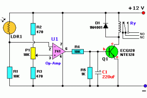
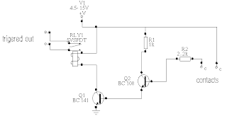
Switch With Relay Schematic

Light Switch With Relay is a series of electronic switches that are controlled by a series of light received. Light Switch With Relay circuit can be used to control lighting automatically, so the lights can automatically turn on when the room light or the region began to decrease. Limit of light used to activate the electronic switch in the circuit Light Relay Switch With This can be set via the potentiometer P1. P1 setting is basically a light reception sensitivity settings. Light Switch With Relay circuit uses the LDR as the light sensor and an IC 741 as a comparator and reference voltage sensor, relay driver transistor Q1 as as an electronic switch. A complete range of Light Switch With Relay is as follows.
Switch

Circuit Light Relay Switch With diats a light switch that will be active when the sensor does not receive light, if you want to turn the tables (the active switch when the sensor receives light) it can be done by reversing the position between the LDR and R1. Diodan D1 serves to avoid the effects of EMF or sparking of the relay coil. The circuit is simple and easy to make, I hope to provide ideas and descriptions in the manufacture of a controlled light switch. Hopefully useful.
Read More..

Microphone Pre Amplifier 9 12Volt Discrete

MicrophoneMicrophone Pre-Amplifier 9-12Volt Discrete

This is a microphone pre-amplifier ambit that use detached components. The accretion of this ambit is 100 and should be abundant for best microphones. It is set by the arrangement of the 10k resistor to the 100R. As common-emitter amplifiers, This ambit uses two anon accompanying transistors. Here is the schematic diagram of circuit:

Please note that this ambit has no bent voltage source, so you can’t use with condenser blazon microphones. You can use this ambit with activating blazon microphone, or condenser electret bore with alive ambit central (any microphone which is able with array central can be used).

Read More..

Doubler Digital Frequency circuit

Doubler Digital Frequency circuit includes a simple and easy to understand. Digital Frequency Doubler circuit application contained in the system electronics such as audio-producing organ, or keyboard. The function of this series Digital Frequency Doubler for multiplying two input frequencies.

The process of multiplying 2 on scales in an organ in principle is like this series Digital Frequency Doubler. Example of rising to a ringing tone DO RE then electronically technique in it is by multiplying the two frequency bands such as this series Digital Frequency Doubler.
Digital Frequency Doubler.
Read More..

DC motor driver with H Bridge IC L293D

IC H Bridge DC motor driver L298 has two H-Bridge circuit in it, so it can be used to download the drive two DC motors. H Bridge DC motor driver L298 each can deliver currents up to 2A. However, in use, the H Bridge DC motor driver L298 can be used in parallel, so the ability to deliver the H Bridge DC motor driver L298 flow into 4A. The consequences of the installation of H Bridge L298 DC motor driver with the parallel mode, you need 2 pieces Bridge H L298 DC motor driver to control two DC motors using H bridge DC motor driver L298 in parallel mode.

H Bridge Pin IC L298 DC motor driver which is connected in parallel operation mode:
* OUT1 connected to OUT4.
* OUT2 OUT3 linked.
* IN1 is connected to IN4.
* IN2 connected to IN3.
* ENABLE ENABLE A linked to B.


DC


OUT1/OUT4 and OUT2/OUT3 associated with DC motors to be controlled.

Please note that the output of the L298 does not have a safety diode. Thus, the need to add two diodes - flyback diodes, with appropriate current capability, at any point output.
Read More..

Monday, November 17, 2014

STV9380 and STV9381 Vertical efficient

STV9380 and STV9381 is a vertical ic-out which very efficient, so it does not require cooling (heat sink) as the vertical ic is generally. This circuit works the same way as most other vertical ic, except at the amplifier end only. Amplifier section works at the end of class D (this is different to the generally vertical ic which working on a class AB). 
STV9380 and STV9381
Vertical signal input by the "MODULATOR" changed its form to first become a form of "pulses" box before it is reinforced by the end of the transistor. Here transistor "amplifier end" work as like "switching transistor". Output result is a strengthening of which pulses of the box is then returned into regular shapes such as vertical signal using an LC fillter (capacitor and filter coil) . Requires IC supply voltage (+) 16V and (-) 16V STV9380 is able to produce pulses of the vertical 2.5 APP (Ampere pitch to peak) and STV9381 3 APP.

STV9380 and STV9381 Vertical efficient

Read More..

Multiplexer with TTL IC 74251

Actually you can not bother to design a multiplexer using logic gates because it has many special IC which functioned for a multiplexer.

One of the TTL ICs from the family that you can use to fulfill the function of a multiplexer is IC 74 251. At the IC there are 8 input channels and 3-bit selector and the other lane as a control reset and inverting output. As a note if you are using TTL ICs for your electronic circuit, the voltage supply that is allowed a maximum of 5 volts. So you can be more familiar with the workings of this multiplexer ic, IC74251 consider the truth table below:


C
B
A
G
Y
W
X
X
X
1
Z
Z
0
0
0
0
D0
D0’
0
0
1
0
D1
D1’
0
1
0
0
D2
D2’
0
1
1
0
D3
D3’
1
0
0
0
D4
D4’
1
0
1
0
D5
D5’
1
1
0
0
D6
D6’
1
1
1
0
D7
D7’
Z = High impedance (off)
D0,D1…D7 = Representing the output of the input lines D

Read More..

Applications for the Matrix Keypad MCS51 Hexadecimal

Hexadecimal keypad matrix can be created with a microcontroller by using the parallel port MCS51. Hexadecimal keypad matrix system is working by reading the data on tiab line through each column or vice versa depending on the program. To make enough Hexadecimal keypad matrix with 1 port MCS51 microcontroller. With 1 parallel port, the microcontroller can be made Matrix Keypad Hexadecimal 4 columns and 4 lines or so-disebud with 4 × 4 matrix keypad. Hexadecimal Keypad Matrix 4 × 4 is in pernacangannya will provide data Hexadecimal 0 - F.
Applications
Parallel port for MCS51 Microcontroller Matrix Keypad
The parallel port is part of the most widely used microcontroller. Ranging from things very simple for example to turn on the LED or read button, used also to form a hexadecimal keypad, to control the stepper motor and connecting the microcontroller to the printer parallel.

In general the parallel port is said to be a means of input / output that can be used to transfer data several bits (typically 8 bits) once gus through lane (feet IC) prepared for it. The path are numbered from 0 to 7, in accordance with the serial number of bits in the accumulator that was used to trasfer data to / from the parallel port. For example, the accumulator is used to receive data from Port 0, then the line number 0 of Port 0 (usually abbreviated as P0.0) will be transferred to the accumulator bit number 0 (usually abbreviated as A.0).

Almost all microcontroller IC legs can be used as a parallel port. AT89C2051 legs 20, 15 feet can be used as a parallel port. AT89C51-footed 40 of them 32 feet can be used as a parallel port.

Nevertheless, there is also a parallel port that does not consist of an 8-lane, for example, Port 1 of AT89C2051 only consists of 7 lines, numbered ranging from P1.0 to P1.7, P1.6 but no. This sort of thing is usually caused by the IC legs are available are not sufficient to contain all relevant path parallel port is complete.

All lines on the parallel port (except Port 0) MCS51 equipped with about 50 kOhm resistance, corresponding to a path connecting Vcc resources. On chip AT89C1051, AT89C2051 and AT89C4051, Port 1 path 0 and 1 (P1.0 and P1.1) are not equipped with these detainees, as a result if both paths are used as outputs must be added detainees outside AT89C2051, which connects the pathways to a power source Vcc.

4 x 4 Matrix Keypad Hexadecimal
Matrix Keypad 4 × 4 is an arrangement of 16 buttons form the keypad as a means to enter into the microcontroller, although the number of buttons there are 16 but only require an 8-lane parallel ports, as shown in the picture below.

In the circuit in the image above, each button connects an output line (K1, K2, K3 or K4) into a line input (B1, B2, B3 or B4), as described in detail in the lower right circle images, buttons "A" connecting path to the lane B4 K1. Working from a series of keypad is fully implemented with the software.
Read More..

50W car audio amplifier schematic

Car power amplifier uses SI1050GL IC as the main amplifier. The output power 50 Watt 8 ohm mono impedance. Up to 25 Volt DC voltage. with source voltage of this amplifier car battery has to work.


Minimum of 12 Volt battery voltage, less than a sound or audio is issued less than the maximum and less good. You can assemble  this circuit amplifier with a schema like this.
Part List
R1 = 100K
R2 = 1R
C1 = 2.2uF
C2 = 22uF
C3 = 100uF
C4 = 0.1uF
C5 = 100uF
U1 = SI1050GL
If you want to make stereo amplifier , you must required multiply the two of components.

Read More..

Water to activated Relay circuit


Water
Water to activated Relay circuit
Read More..

Sunday, November 16, 2014

Magnetic Switch Circuit

Magnetic switch is a circuit which can respond to magnetic fields that were around the sensor. The series of magnetic switches uses sensors in the form of limit switches that provide an additional metal plate that can respond to a magnet. Magnetic switch circuit is made ​​with an NE555 monostable multivibrator and a flip-flop togle from IC CD4013. The series of magnetic switches uses 12VDC supply voltage and the magnetic circuit is mounted indicator switch which serves to give a signal when the sensors respond to magnetic fields using the LED D1. Here is a complete range of magnetic switches.

Magnetic

If the limit switches (sensors), active (connected) then it will get multivibrator NE555 triger signal and provides output pulses to be used to provide input signals to the flip-flop togle Relay K1 and active. Then when the sensors (limit switches respond to the magnetic field again, the multivibrator will give togle pulse as input to the flip-flop relay K1 and non-active.

Read More..

Magnetic Proximity Switch Circuit

Here is the circuit diagram of a magnetic proximity switch that finds a lot of applications in abounding fields.The ambit is based on a alluring reed switch(S1) as the adjacency sensor. A monostable multivibrator based on NE555 (IC1) and a toggle cast bomb based on CD4013 (IC2) does the blow of the circuit.

When a allurement is accomplished in adjacency of S1 it closes to accord a abrogating activate at pin 2 of IC1.The achievement of IC1 goes top for a time determines by R2 and C2.This clocks the IC2 active as a toggle cast flop.The achievement (pin 1 ) of IC2 goes top and the transistor Q1 is biased to ON.The broadcast is activated and so do the accessories affiliated to the relay.The LED D1 glows if IC1 is triggered.

When a allurement is accomplished in adjacency of S1 it closes to accord a abrogating activate at pin 2 of IC1.The achievement of IC1 goes top for a time determines by R2 and C2.This clocks the IC2 active as a toggle cast flop.The achievement (pin 1 ) of IC2 goes top and the transistor Q1 is biased to ON.The broadcast is activated and so do the accessories affiliated to the relay.The LED D1 glows if IC1 is triggered.
Read More..

Saturday, November 15, 2014

ELECTRONIC FUSE CIRCUIT

The Fuse is a type of electrical equipment to the poor. Because it sacrifices itself. To protect the safety devices in the circuit. In the case of current flow in circuit too much. Until it melted. Due to an error in the circuit. The structure is a glass cylinder with an alloy of lead wire is connected between the two terminals. When the current through it too much, Alloy within is temperature rises until the melting. Makes wires were cut off.

In some experiments a electronic circuits require a fuse protection. Circuit may be difficult. Because, often short, to change the fuse every time. Thus wasting time.

To solve this problem, we Build this electronic fuse, so instead of plain fuses. By it can cut off the current immediately. When a short circuit as well. But can work immediately. Just press the reset button only. Convenient and economical than using plain fuses. We also can set up and cut off current as you want.

How the electronic fuse works?

The electronic fuse that we use in this project is in Figure 1. Which will include important devices are transistors of 2 pcs, and Electronic devices in thyristors type of 1 piece works, together.


In the Figure 1, This project across between the power supply and load that will be applied immediately, When a input of electronic fuse to the power supply. Then, Q1-transistor conduct current causes a Q2-Darlington transistor works as well, collector and emitter will conduct current by resistor R3 out to the Load that connected with the pin output(K2).

When the load use current will cause has a voltage across R3. If load use high current will cause voltage across R3 too much as well. As Ohm’s law. And When Load use current until voltage across R3 more than 0.6 volts. Then, this voltage will trigger to SCR1 conduct current.

This SCR or silicon controlled rectifier will works or conduct when get trigger at pin gate (G), and It will bring current indefinitely.
Although no trigger it.

How to stop the Works is remove its power supply there. We will bring this feature to use in our circuit. When voltage across R3 over 0.6 volts, the SCR1 will conduct , makes voltage at base of Q2 drop to level that transistor cannot conduct high current.

From the original. collector and emitter has conduct current into stop, causes current flow to load next step, until push reset switch-S1 ,to separate SCR1 out of circuit. After that Q2 will start conduct current again.

In the section of Q1, LED1 and R2 there, will be together serving as a constant current circuit. To Q2 conduct when Normal conditions, and stop current to Q2, when SCR1 conduct current to ground.

Determination current of fuse

The current of fuse that you want to cut off circuits, can easily set easily from changing R3 which is a current detector. When we use Ohm’s law, which circuit will cut current when voltage drop across R3 is 0.6 volts.

Based this condition, we can find the right resistor with the following formula.
R3 = 0.6/I ….(1)

We set I is the current that want to start cutting circuit. (Is measured in amps.)

For example want to start cutting at 500 mA will must connect R3 are :

R3 = 0.6/0.5 = 1.2 ohms.

Thus, If you need the electronic fuse cut current at 500 mA, it must use R3 of 1.2 ohms. The rate watt resistant of resistor values (P) from:

P = 0.6x current value (amperes) ….(2)

Will have P = 0.6×0.5 = 0.3 watts

So must select the Resistor of 1.2 ohms , the power rate is 0.3 watts But resistor size 0.3 watts no selling, so use 0.5 watts instead.

From example can easily define current of electronic fuse. Who Those who want to use fust in others currents, can It can be calculated from equation (1) and (2) to calculate Resistance (R3).

But should be less than 1 Amperes, because that Darlington transistor unbearable. And should be used only in the voltage of 10-25 volts.

The components List

Resistors ¼ W + 5%
R1———————4.7K
R2———————68ohm
R3——————— see text

Semiconductors
Q1—————-BD140___100V 1.5A PNP transistor
Q2—————-BD679___100V 2A NPN transistor
LED1 (Light emitting Diode) Red 5 mm
SCR1————-TIC106E

Other parts
K1-K3 terminal into PCB
S1 Switch, press the off, released stick, etc.
Read More..

Friday, November 14, 2014

Voltage Doubler Circuit Using NE555

The circuit diagram of a very simple voltage doubler using NE555 timer is shown here. Here IC NE555 is wired as an astable mutivibrator operating at around 9KHz. The base of the two transistors (Q1 and Q2) is shorted and output of the astable multivibrator (pin 3) is connected to it. When the output of astable multivibrator is low, Q1 will be OFF and Q2 will be ON. The negative terminal of the capacitor C3 will be shorted to ground through T2 and it will be charged to the input supply voltage. When the output of the astable multi vibrator is high, transistor Q1 will be ON and transistor Q2 will be OFF. The capacitor C4 will be charged to the voltage across capacitor C3 plus the input supply voltage (that is double the input voltage). This is how the circuit works.

This voltage doubler circuit can deliver only up to 50mA output current and above that current limit the output voltage will be dramatically reduced. The actual output voltage will be around 19V for a 12V DC input and also the output voltage will be a bit unstable. Anyway, for low current applications this circuit is well enough.

Circuit Diagram


Important Points

  • The circuit can be assembled on a vero board.
  • The output current should not be allowed to exceed 70mA.
  • IC1 must be mounted on a holder.
Read More..

AM TRANSMITTER

Circuit Description

The heart of this circuit is a FET BFW10 (T1) which works as a feedback oscillator. The frequency of the RF signal can be determined by the oscillator coil L1 and variable capacitor VC1. The audio signal from an amplifier or any audio device such as cassette player, organ, TV etc whose output impedance is 4Ω to 16Ω is fed to the source of FET. The amplitude of the RF wave can be varied by 1 KΩ preset VR1. The frequency adjustments are made through the coil and capacitor C4 and C5. The output of the transmitter is taken through trimmer VC3 to a telescopic or indoor wire antenna. Turn the radio receiver to the transmitter carrier frequency and adjust the volume control of audio input device, VR1 and VC3 to get clear undistorted sound in radio receiver as well to achieve better modulation percentage.

Circuit Diagram

Here is a low-cost, good-stability RF / Am transmitter which uses only one FET.


Parts List

Resistors (all ¼-watt, ± 5% Carbon unless stated otherwise)
•R1 = 100 KΩ
•R2 = 320Ω
•VR1 = 1 KΩ

Capacitors
•C1 = 100 pF
•C2 = 100 µF/16V
•C3 = 0.01 µF
•VC1 = 365 2j
•VC2 = 22p
•VC3 = 70p

Semiconductors
•T1 = BFW10

Miscellaneous
•L1 = MW or SW osc. Coil

Read More..

Thursday, November 13, 2014

TDA2030 18W 18W Stereo Hi Fi Audio Amplifier Diagram Circuit

2 x 18W Hi-Fi Stereo Power Amplifier based around two TDA2030 ICs. It has good input sensitivity, low distortion, good operating stability and full protection against overloads and output short-circuits. It can be used as a booster amplifier for existing small systems or to drive a second pair of speakers besides the ones already connected to the system. The board needs a symmetrical power supply of ±18Vdc/3A and can be connected to loads of 8 or 4 Ohm. Large heat sink is required for this circuit. Diagram shown below indicates only left channel. Make two circuits for for stereo version.Picture of the project:
 18 watt + 18 watt hi fi stereo audio power amplifier circuit schematic diagram
18+18 Watt Hi-Fi Stereo Audio Amplifier Circuit Diagram

Circuit Diagram:
 18 watt + 18 watt hi fi stereo audio power amplifier schematic circuit diagram
Diagram Shows Only One Channel

Parts:R1 = 22K
R2 = 680R
R3 = 22K
R4 = 1R-1w
D1 = 1N4001
D2 = 1N4001
C1 = 1uf-25V
C2 = 22uF-25V
C3 = 100nF-63V
C4 = 100nF-63V
C5 = 100uF-25V
C6 = 100uF-25V
C7 = 220nF-63V
IC = TDA2030If it does not work:
  1. Check your work for possible dry joints, bridges across adjacent tracks or soldering flux residues that usually cause problems.
  2. Check again all the external connections to and from the circuit to see if there is a mistake there.
  3. See that there are no components missing or inserted in the wrong places.
  4. Make sure that all the polarized components have been soldered the right way round.
  5. Make sure the supply has the correct voltage and is connected the right way round to your circuit.
  6. Check your project for faulty or damaged components.

Technical Specifications:
  • Supply voltage = ±18Vdc/3A symmetrical (see text)
  • Current consumption = 3A maximum
  • Input impedance = 500K Ohms
  • Input sensitivity = 250 mV
  • Signal to noise ratio = 80 dB
  • Frequency response = 20 - 20,000 Hz ± 1 dB
  • Distortion = 0.5 % maximum
  • Load impedance = 4 - 8 ohm
Read More..

3000 watt power inverter 12V DC to 230V AC

Circuit Diagram | 3000 watt power inverter 12V DC  to  230V AC

inverter
Circuit Diagram of 3000 watt power inverter 12V DC to 230V AC


Fig. 2: Sine-wave voltage and conventional square wave voltage with both 230 Volt rms


Fig. 3: Square wave voltage with duty cycle 25% for 230 Volt rms ("modified sine")


PCB Layout:3000 watt power inverter

3000w 


Component Placement: 3000 watt power inverter

3000w


fig.: output voltage with no load or inductive load.


fig.: resistor 0,001 Ohm made of high-grade steel sheet metal


Control electronics |12V DC  to  230V AC

fig.: control electronics on strip hole plate (previous version) and PCB of the "professional edition"

Assembly of the mosfet-transistors on the heat sink | 3000 watt power inverter


fig.: heat sink, mosfet transistors, connections.


Final assembly | 3000 watt power inverter 12V DC  to  230V AC


fig.: 1500 VA inverter with 2 parallel transformers and 1000 VA inverter

Source:http://www.qsl.net

Read More..