Showing posts with label digital. Show all posts
Showing posts with label digital. Show all posts
Tuesday, November 18, 2014
Doubler Digital Frequency circuit
Doubler Digital Frequency circuit includes a simple and easy to understand. Digital Frequency Doubler circuit application contained in the system electronics such as audio-producing organ, or keyboard. The function of this series Digital Frequency Doubler for multiplying two input frequencies.
The process of multiplying 2 on scales in an organ in principle is like this series Digital Frequency Doubler. Example of rising to a ringing tone DO RE then electronically technique in it is by multiplying the two frequency bands such as this series Digital Frequency Doubler.
 |
| Digital Frequency Doubler. |

Thursday, October 30, 2014
TDA8551 AF Amplifier With Digital Volume Control Diagram Circuit
The Philips Semiconductors TDA8551 is a small audio amplifier with an integrated volume control. When operated from +5 V, it delivers a nominal output power of more than one watt into 8 ohms. It can also be used over a supply voltage range of +2.7 to +5.5 V, with correspondingly reduced output power. The output volume can be adjusted from –60 dB to +20 dB in 64 steps, using a set of up and down push-buttons. The shared UP/DOWN input for the up and down switches has three states. If it is ‘floating’, which means that both of the switches are open, the volume remains unchanged. A pulse to earth decreases the volume by 1.25 dB, while a positive pulse increases the volume by 1.25 dB.
 When the power is switched on, the internal counter takes on the –20 dB setting. An additional input (MODE) allows the amplifier to be switched from the operating state to the mute or standby state. If this input is held at the earth level, the amplifier is operational. If +5 V is applied to this pin, the TDA8551 enters the Standby mode, in which the current consumption drops from the typical operational level of 6mA to less than 10µA. Finally, the MODE input can be used as a mute input by applying a voltage of 1 t0 3.6 V to this input. This voltage can be provided by a connection to the SCR pin, which lies at half of the operating voltage and to which a filter capacitor is connected.
 The loudspeaker is connected in a floating configuration between the two outputs of the bridge amplifier in the TDA8551. This provides the desired output power level, in spite of the low supply voltage. For headphone applications, which do not need as much output power, you can connect the headphone between earth and one of the outputs, via an electrolytic coupling capacitor. You can make a stereo headphone amplifier in this way, using two TDS8551 ICs. The TDA8551 is housed in a DIP8 package. The SMD version is the TDA8551T, in an SO8 package
 When the power is switched on, the internal counter takes on the –20 dB setting. An additional input (MODE) allows the amplifier to be switched from the operating state to the mute or standby state. If this input is held at the earth level, the amplifier is operational. If +5 V is applied to this pin, the TDA8551 enters the Standby mode, in which the current consumption drops from the typical operational level of 6mA to less than 10µA. Finally, the MODE input can be used as a mute input by applying a voltage of 1 t0 3.6 V to this input. This voltage can be provided by a connection to the SCR pin, which lies at half of the operating voltage and to which a filter capacitor is connected.
 The loudspeaker is connected in a floating configuration between the two outputs of the bridge amplifier in the TDA8551. This provides the desired output power level, in spite of the low supply voltage. For headphone applications, which do not need as much output power, you can connect the headphone between earth and one of the outputs, via an electrolytic coupling capacitor. You can make a stereo headphone amplifier in this way, using two TDS8551 ICs. The TDA8551 is housed in a DIP8 package. The SMD version is the TDA8551T, in an SO8 package
Wednesday, October 29, 2014
CD4017 Digital Dice Circuit
A electronic acquaintances was seeking a star as circuits in vogue your at no cost point in time,a shameful and uncomplicated to made.This dice digital circuit would occur a favorite of all and sundry, by using it to flaunt the records. As you switch to a spin button before it like is tossing a dice. Looks like a random form normally.

A focal point of this circuit,an a secure oscillator 1Khz with IC 555 and RC networks,it resolve be located output to IC2 is Decade counter IC - 4017. After I focus inedible the spin switch, it will be converted to a binary input with a diode matrix D1-D9 (1N4148 before numeral 1N914) and so therefore untouched to a 7 segment put on show with a decoder drive IC refusal. CD4511 (IC3). The brightness of the numeric display, may well occur customized by adjusting the quantity of R3.
Thursday, October 16, 2014
Super Digital Combination lock Circuit Diagram

The circuit above above makes use of the CMOS 4017 decade counter IC. Each depression of a switch steps the output through 0– 9. By coupling the output via an AND gate to the next IC, apredefined code has to be input to create the output. Each PBSswitch is debounced by tw1o gates of a CMOS4001 quad 2-input NORgate. This ensures a clean pulse to the input of each CMOS4017 counter. Only when the correct number of presses at PBS Awill allow PBS B to become active. This is similar for PBS C andPBS D. At IC4, PBS D must be pressed 7 times. Then PBS C is againpressed 7 times, stepping from output 1 to output 8. The ANDgate formed around CMOS4081 then goes high, lighting the LED. TheReset switch can be pressed at any time. Power on resetis provided by the 100n capacitor near the reset switch. Below isa picture of one that I made about 15 years ago:

Unfortunately, this board was part of a much larger project containing multiple power supplies. One day whilst working on another circuit , I slipped with a wire and splashed 24volts DConto this board. There was a small spark, and puff of smoke before all this chips were cooked! If anyone does consider building such a circuit, then my advice would be to stop and lookin your local electronic parts catalogue. There are now dedicated combination lock IC`s with combinations many time sgreater than this circuit. Incidentally the number of combinations offered here is 10 x 10 x 10 x 10 x 9 = 90,000.Check out Dean White`s Electronic Gadgets, on the Electronic Sites Alliance web ring, he also has a combination lock circuit.
Tuesday, August 26, 2014
Digital Stop Watch
A digital stop watch built around timer IC LM555 and 4-digit counter IC MM74C926 with multiplexed 7-segment LED display.MM74C926 consists of a 4-digit counter, an internal output latch, npn output sourcing drivers for common cathode,
7-segment display and an internal multiplexing schemary with four multiplexing outputs.The counter advances on negative edge of the clock. The clock is generated by timer IC LM555.The schema works off a 5V power supply. It can be easily assembled on a general-purpose PCB. Enclose the schema in a metal box
with provisions for four 7-segment displays, rotary switch S1, start/stop switch S2 and reset switch S3
Testing
First, reset the schema by pressing S3 so that the display shows ‘0000.’ Now open switch S2 for the stop watch to start counting the time. If you want to stop the clock, close S2. Rotary switch S1 is used to select the different time periods at the output of the astable multivibrator (IC1).
Thursday, August 21, 2014
SONY PRS T1 DIGITAL BOOK READER DISASSEMBLE PROCEDURE
Sony PRS-T1- DIGITAL BOOK READER US Model; Canadian Model; AEP Model & UK Model _ Disassemble Procedure
Click on the pictures to Zoom In
.jpg)
Confirm the operation after pressing the button of the main unit bottom without fail when soldering the BATTERY ASSY (BAT1) to the MAIN board.


MAIN BOARD

CASE FRONT ASSY

BATTERY ASSY (BAT1)

Saturday, August 9, 2014
5 Watt Digital Power Supply
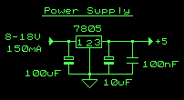
5 Watt Digital Power Supply is a small +5V power supply, which is useful when experimenting with digital electronics. Small inexpensive wall tranformers with variable output voltage are available from any electronics shop and supermarket. Those transformers are easily available, but usually their voltage regulation is very poor, which makes then not very usable for digital schema experimenter unless a better regulation can be achieved in some way. The following schema is the answer to the problem.
This schema can give +5V output at about 150 mA current, but it can be increased to 1 A when good cooling is added to 7805 regulator chip. The schema has over overload and therminal protection.
This schema can give +5V output at about 150 mA current, but it can be increased to 1 A when good cooling is added to 7805 regulator chip. The schema has over overload and therminal protection.
Subscribe to:
Posts (Atom)